High Speed Magnetic Field Pulsar

The goal of the project is to design and fabricate a device that can speed up signals in optic cable applications via the use of high speed magnetic pulses and magneto-optic material. The device will be capable of producing magnetic field pulses greater than or equal to 500 gauss within 100 nanoseconds, will be powered by a source voltage of less than or equal to 15 Volts DC, and will be less than 3.5” by 2” in physical size. Given the design requirements and resources from the previous iterations of this project, we plan to create an improved design including a reduced rise time of 10ns, functional programmable control of the magnetic field generation, reduced overall noise, and increased stability.
Responsibility
I’ve learned a lot in this project and it’s mainly about the components we had to source. An area I was focused on is the MOSFET which is crucial in determining the characteristics of the magnetic pulse we’re going to get. I’ve had to read a lot of datasheets on the components previous teams used and look for a MOSFET that’s potentially better such as GaN MOSFETs. I’ve also had to learn a lot about simulation of non ideal components through Advanced Design System (ADS) and finding ways add on to previous circuits so that we can achieve get more accurate measurements and get less noise in the waveform.
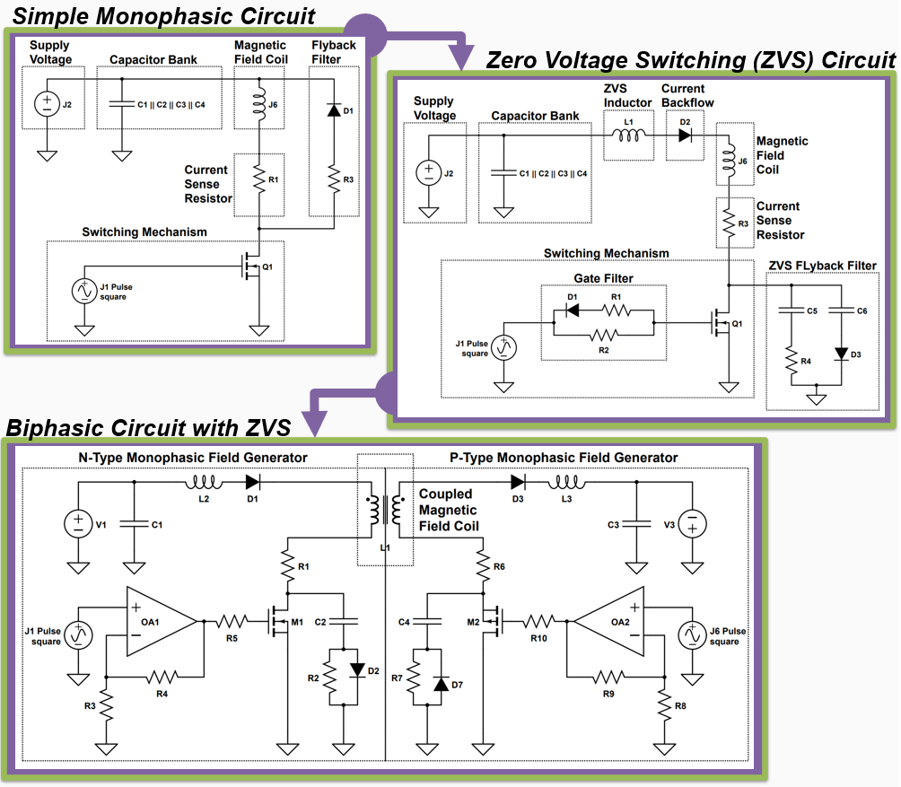
I lead the team in creating a circuit design that uses ideas such as zero voltage switching for less power loss in our circuit and a biphasic design which will remove residual magnetic field in the coils for a faster rise time. I was instrumental in my team’s success of this project because I am able to grasp new concepts easily and explain it to them in a way that was easier to understand because external resources such as research papers were highly technical. I am also very dedicated in my work in the way that I would spend hours in the lab meticulously testing our circuits for its flaws, limits, and to really understand what each component adds to our circuit. For example, we found that parasitic capacitance in our MOSFETs was leading to a lot of instability in our waveforms, but it can also be used to our advantage through zero voltage switching which can significantly reduce our power loss since we were putting 20-40 Amps of current through our MOSFETs to achieve the 500 gauss magnetic field.
Application
This device will be used in networking systems to increase the bandwidth of the system by using magneto-optic switching. This concept uses Faraday effect, which is a change in the polarization of the travelling EM wave caused by optic cable caused by an outside EM field. Since this switching is faster than current systems used, we can achieve a larger bandwidth in our network. The larger bandwidth will be able to host more users, thus being more cost effective in theory